Are you fascinated by things that are really small? Isn't it amazing that something as small as an ant would have so much going on their bodies that make them work. And thanks to Macro lens, we can capture all those details pretty easily. Going smaller, we have bacteria. These single cell organisms are many times smaller than us, yet with the help of optical microscope we can study what’s inside them, their nuclei, cell walls, movements, everything. But what about atoms. Atoms, being the basic constituent of everything around us, is of course very very tiny. Can we ever hope to see atoms? Well, thanks to modern technologies, we can. Sort of. I say sort of, because atoms are very small. Their diameter, of the average of 0.1 nm to 0.5 nm (each nm or nanometer is 10-9 metres, or 0.000000001 m) is much smaller than the wavelength of visible light (~400 – 800 nm). This means that our eyes will never be able to physically see light reflecting off an atom. However, there are other means, all of them rely on the interaction between an atom and electrons. Today, I will be introducing you to one of these powerful microscopy techniques – Scanning Tunnelling Microscopy (STM).
微观的世界是多么的奇妙!像蚂蚁这么细小的动物,也是五脏俱全。利用微距镜头,我们可以很简单的去捕捉它们的不同形态和细节。再微小一些的细菌,我们也可以用显微镜去研究它们的构造。哪么原子呢?我们可以看到原子吗?答案是可以的!不过,我说的看不是用眼睛直接看,因为可见光的波长是400纳米(1 纳米 = 0.000000001 米) 到600纳米,比只有0.1纳米的原子大得多,所我们是不能光学上看见原子的。可是我们可以用原子和电子的相互作用来间接的观察原子。这些所谓的电子显微镜都可以观察光学显微镜看不到的东西。今天我要跟大家介绍的是扫描隧道显微镜(STM)

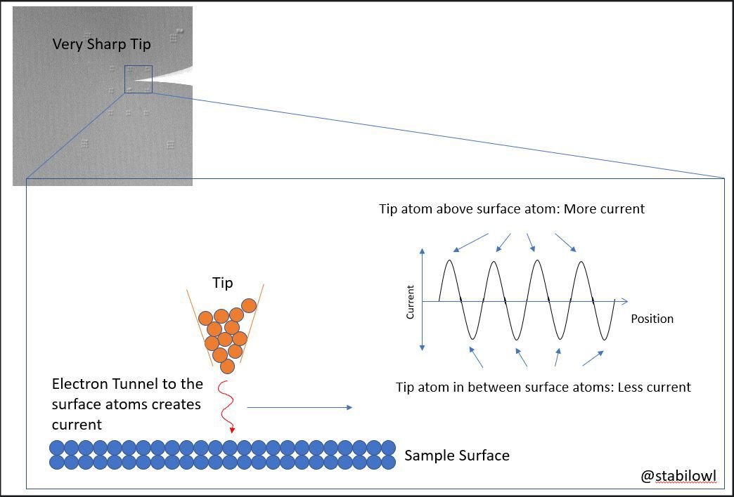
A scanning tunnelling microscopy uses a very fine metal tip, usually made of Tungsten for is hardness. The tip is machined so sharp that at the end of the tip, it would only have a single atom. Then, we would lower this tip to a position very close to the sample surface, but not touching, so that there is a gap between the last atom on the tip, and the atoms on the surface of the tip. Now if we apply a voltage, the atom on the tip and on the surface will be close enough for electrons to jump, or in more technical terms, tunnel, from the tip to the surface. We therefore get a current. And as the tip scan across the surface, the current becomes larger when the tip atom is directly on an atom (as the distance to a surface atom is minimised), and smaller when the tip atom is in-between two atoms. Therefore, if we convert this current map into a visual map, we will be able to see with our eyes where the atoms are located – we are essentially seeing atoms!
STM 用一支很尖很尖的探测针,针头尖得只有一粒原子。当把针头接近样本表面然后施加电压,针头原子的电子可以跳过真空(穿隧)到达样本表面而形成电流。如果用探测针在样本表面上下扫描,就会发现,当针在一粒原子上方,电流会增加。针在二粒原子之间则反之。把这个电流变化变成一个视觉图,就可以变相的看到原子了!
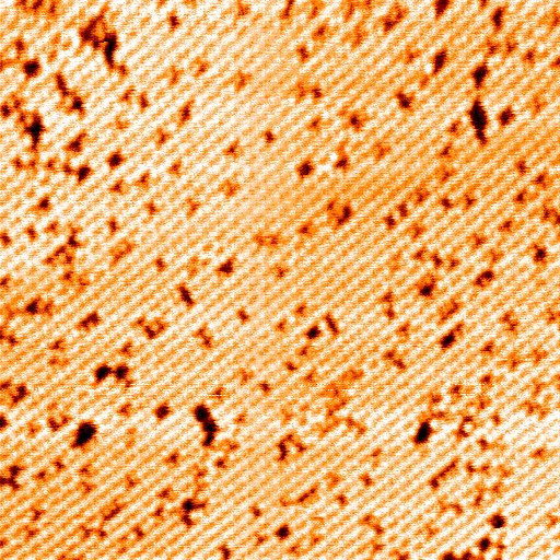
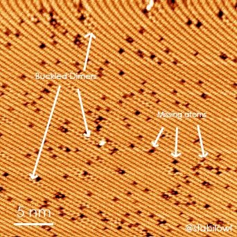
Here is an image of the surface of a Silicon Si(100) sample using STM that I took when I was working as a postdoc at UNSW. You can clearly see rows in the image which are essentially rows of atoms, and if you look closely, you could almost make out each single atom. The dark holes on the surface is where a Si atom is missing on the first layer of the surface. The whole of the image is only 30 nm across, which mean we are looking at something very very tiny! You can also see that some of the atom rows seems to be wriggling. That’s because Si atoms interacts in such a way that they don’t actually form straight rows, but they are bent. If the bending is opposite each other in each consecutive pair of Si atoms or dimers, the atomic rows would essentially look like it is wriggling.
这张图片是我在UNSW工作时所取。图为硅(Si)晶片的表面。我们可以看到一排排的硅原子列。图中看到像洞的东西就是晶片表面上少了粒原子的地方。图中还有一些波浪形的原子列。这是因为硅原子跟硅原子之间的键不是直而是有角度的。如果相反角度的原子对并列在一起看上去就是波浪形了。

Here is another image of a silicon surface. This time, you can see the individual atoms (actually, pairs of atoms) even more clearly now. You can also see there is a brighter and darker part of the image, and at these two parts, the atomic rows run perpendicular to each other. Each of these area is called an atomic step. All surfaces generally have steps like this, where each step is 1 atom higher compared to the step below. These surface atomic steps are very important for material deposition process. A zoomed out image of the atomic steps on this surface can also be seen below.
这是另外一张硅晶体表面图,单个原子对在这图里看得更清楚了。我们还可以看见图中的左面比右面要亮。这是因为左面比右面要高出一个原子。这就是所谓的原子阶梯。所有晶体的表面都是由很多原子阶梯所组成。下面的右图可以看见这些阶梯的缩小图。
Here we have a series image of the same Si surface, with more and more Si deposited on top. We can see that small islands start to grow randomly on the surface, first as rows of atoms, but then as we put more Si on the surface these islands grows, but generally on the same atomic step. Only later in the process that we start seeing islands that have more than 2 atomic steps. By using STM to study the growth of these Si Island at different stages, we are able understand the island dynamics and better tune the process to adjust the properties of the newly deposited material.
最后一组图是硅晶体生长的过程,程现了硅晶体五秒,十秒和十五秒的沉淀。可以看见原子像岛一样一层层的生长。用STM观察晶体的生长过程有助我们研制和优化材料的结构和程序。
STM is a very important tool in studying surface atom dynamics, in a branch of science that is known as surface science. Surface science is very important in understanding chemistry, how different materials interact with each other, and how new materials form. Because of its ability to image in the atomic scale, STM is also a very useful tool to study quantum phenomena and even to design quantum devices. In my next post, I will show you how we use STM as a tool to move atoms to make very small, atomic scale devices.
STM 是表面科学一个很重要的工具。我们用STM去研究不同原子在不同表面上的动态和相互物理和化学作用,从而去研发新材料。STM还可以用来研究很多不同的量子效应,或者用来设计量子设备。下一次我会为大家介绍怎样用STM来移动原子去制造原子设备!
